
This is the square wave oscillation circuit which used NE555. 555 was developed as the IC for the precision timer. It is compactness (DIP 8 pins) and it is simple composition. It is often used for the timer circuit, the oscillation circuit because of precision well the operation

Three resistors are connected with the inside in series and the power supply voltage(Vcc) is divided in 3. This composition is an excellent point. 1/3 with power supply voltage is applied to the positive input terminal of the comparator (COMP1) and the voltage of 2/3 is applied to the negative terminal of the comparator (COMP2). When the voltage of the trigger terminal(TRIGGER) is less than 1/3 of the power supply voltage, the S terminal of the flip-flop(FF) becomes H level and an FF is set. When the voltage of the threshold terminal(THRESHOLD) is more than 2/3 of the power supply voltage, the R terminal of the FF becomes H level and an FF is reset.
The condition immediately after the turning on
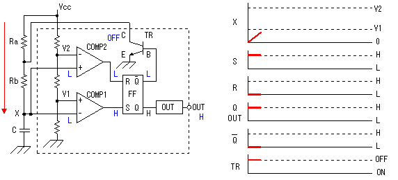
Immediately after a power supply voltage is supplied, as for the FF, the Q becomes H and
Output's reverse (1)
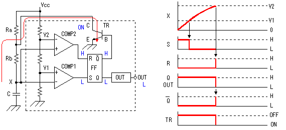
When the voltage of the X point crosses V1 of COMP1, the output of COMP1 becomes L. However, this change doesn't change the condition of the FF. The output of COMP2 becomes the H condition when the voltage of the X point rises more and reaches V2 of COMP2. With this, the R terminal of the FF becomes H and the output state of the FF reverses. The Q becomes the L condition and
It is only in a little time that the R terminal of the FF becomes the H condition.
Output's reverse (2)
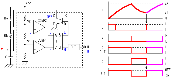
Because TR becomes ON, as for the electric charge of capacitor(C), it continues the discharge and the voltage of the X point falls. When the voltage of the X point becomes equal to or less than V1 of COMP1, the output of COMP1 becomes the H condition and the S terminal of the FF becomes the H condition. This changes the Q of the FF to H and
When charging (accumulating the electric charge) capacitor(C), the electric current flows through Ra and the Rb and in case of the discharge (missing the electric charge), it passes only the Rb. So, the time of the charging and the time of the discharge are different. By making the Rb compared with Ra big, the difference of both becomes small but can not make the same at all. To make the same, it is good if Ra is 0 ohm, but in the case, Vcc is directly connected with TR and TR has broken. Don't make Ra = 0 ohm absolutely. If doing the ratio of Ra and the Rb by several times, in case of the practical use, there is not a problem.
Timer IC ( 555 )
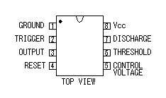
There are a lot of second sources in 555 because the circuit is simple and is with a good performance.
The second source is the IC to be selling by the similar function from the other manufacturer. The pin arrangement is the same and it is possible to replace.
There is an energy saving type of the CMOS, too
Resistor
As the resistor, I am using the type that the permission electric power is 1/8 W. More than 1/8-W resistor can be used, too. In the case, the size of the resistor becomes big. This time, 1/8-W resistors are used to make a circuit compactly.
Capacitor

A multilayer ceramic capacitor is used for the capacitor to decide an oscillation frequency. The capacitor with good temperature characteristic should be used for this capacitor. The capacitor with good temperature characteristic is the capacitor where little change of the value occurs even if the ambient temperature changes. The polypropylene capacitor is a capacitor with good temperature characteristic. However, the precision of the oscillator doesn't become good even if only the temperature characteristic of the capacitor is excellent.
IC socket
The IC can be put to direct to the printed board, too. This time, a socket is used.
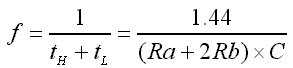
Calculation of the frequency of 555 oscillator
The oscillation frequency of this oscillator is fixed by the value of capacitor (C) and resistor (Ra) and resistor (Rb).
Roughly oscillation frequency can be calculated by the following formula.
Because there is an error of the part, the oscillation frequency of the actual circuit is sometimes different from the calculated value little.
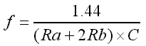
Unit f : Hz / C : Farad / Ra and Rb : ohm
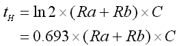
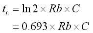
It is possible to calculate by the following formula in the time that the output becomes H level and the time which is made an L level.
|
It is as follows when calculating at the value of the circuit this time.
|
The oscillation frequency of the made circuit was to 1,114 Hz be with the +5V power. The difference with the calculated value seems to be the factor that the error of the part is big. I attempted to change 555 (different manufacturer) but the oscillation frequency was the same approximately. |
I measured the change of the oscillation frequency by the change of the line voltage.
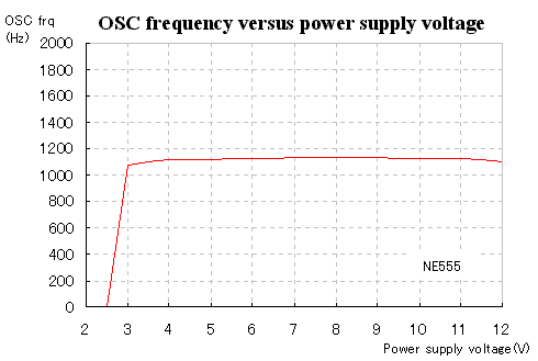
The oscillation frequency is stable at more than +3V voltage.
It is the most stable in the voltage for 7V to 9V and it is the change of about ±1Hz(±0.1%).


No comments:
Post a Comment